21.2 Vortex Processor Digital I/O Ports
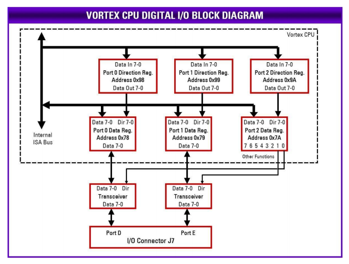
The Vortex processor has an integrated digital I/O (GPIO) circuit with 5 8-bit ports. Two of them (ports 0 and 1) are available for use as general purpose digital I/O on Helios and are identified as ports D and E. These ports are accessible on I/O connector J7. The other 3 ports (2, 3, and 4) are reserved for other functions and should not be disturbed except as described in this manual. All GPIO ports are addressable in the ISA bus I/O space.
Each GPIO port has a data register and a direction register. Before the port can be used, the direction register must be configured. Each port is isolated from the I/O connector via an 8-bit bi-directional transceiver to protect the processor chip and provide enhanced output current capability. These transceivers require all 8 bits to be the same direction. Therefore each GPIO port direction register must be configured as either all input or all output.
The two 8-bit transceivers must also have their direction configured to match the intended direction of the two GPIO ports. To avoid possible conflicts in the circuitry with the processor and the transceiver driving their data lines simultaneously, the first step is to configure the direction of the transceivers.
The I/O addresses of the GPIO data and direction ports are as follows:
Direction Control Register
The GPIO port 2 direction register at address 0x9A should always be set for all output mode by writing 0xFF to it. This is the default setting, so no change should be required. Then the DIO port D/E direction control data can be written to bits 1 and 0 of address 0x7A. Bit 1 controls the direction for port E, and bit 0 controls the direction for port D. A 1 sets the port for output, and a 0 sets the port for input.
The data written to the direction control register should be confined to bits 1 and 0, because the other bits are used for the serial port 1 and 2 protocol selection and should not be disturbed. The bits are set by first reading the current register value, modifying the selected bit or bits, and then rewriting the data to the port. The example C code below shows how to do this:
dir = inp(0x7A); // read current port 2 register data
dir &= 0xFE; // example, clear bit 0 to configure port D as input
dir |= 2; // example, set bit 1 to configure port E as output
outp(0x7A, dir); // write new data to port 2 register
Port Direction Registers
To set a port to output, first set the corresponding port 2 direction bit at address 0x7A to 1, then set the port 0 direction register 0x98 or port 1 direction register 0x99 to 0xFF.
To set a port to input, first set the port 0 direction register 0x98 or port 1 direction register 0x99 to 0x00, then set the corresponding direction bit at port 2 / address 0x7A to 0.
The only valid values for the port 0/1 direction registers are FF and 00, since all bits in the port must be set to the same direction due to the presence of the transceiver chip between the port and the I/O connector. The sequences above are important to avoid conflicts with both the CPU chip and the transceiver chip driving their connection simultaneously.
Port Data Registers
Once the direction registers for ports D and E are configured, the ports can be read or written as required at addresses 0x78 and 0x79. Reading a port set for input mode will return the data on the corresponding I/O connector pins. Writing a port in input mode will have no effect. Reading a port in output mode will return the value last written into that port. Writing a port in output mode will send that data to the corresponding I/O connector pins.
The example C code below shows how to configure and use ports D and E. In this code the example configuration above is assumed to have already been executed, namely port D = input and port E = output.
outp(0x98, 0); // set port D to input
outp(0x99, 0xFF); // set port E to output
ddata = inp(0x78); // read data from port D
edata = 0x12; // set port E to 00010010
outp(0x79, edata); // write new data to port E
Last updated