7. IO CONNECTORS
This page describes the pinouts of various connectors available with the Floyd SC daughter card.
7.1 Daughter Board Expansion (J5)
Expansion carrier pinout is given below:
40 | V_VIN |
39 | V_VIN |
38 | V_VIN |
37 | V_VIN |
36 | V_VIN |
35 | V_VIN |
34 | V_VIN |
33 | GND_DIG |
32 | PCIE_XNX_DB_RST# |
31 | GND_DIG |
30 | PCIE_XNX_DB_TX_P |
29 | PCIE_XNX_DB_TX_N |
28 | GND_DIG |
27 | PCIE_XNX_DB_RX_P |
26 | PCIE_XNX_DB_RX_N |
25 | GND_DIG |
24 | PCIE_XNX_DB_CLK_P |
23 | PCIE_XNX_DB_CLK_N |
22 | GND_DIG |
21 | USB2_D1_DB_N |
20 | USB2_D1_DB_P |
19 | GND_DIG |
18 | USB3_TX1_DB_P |
17 | USB3_TX1_DB_N |
16 | GND_DIG |
15 | USB3_RX1_DB_P |
14 | USB3_RX1_DB_N |
13 | GND_DIG |
12 | PCIE_XNX_CLKREQ_DB_3P3# |
11 | DB_PRESENT_3P3 |
10 | GND_DIG |
09 | SDIO_CLK |
08 | SDIO_D0 |
07 | SDIO_DB_D1 |
06 | SDIO_D2 |
05 | SDIO_D3 |
04 | SDIO_CMD |
03 | GND_DIG |
02 | SDIO CD |
01 | PCIe Wake |
Note: The connector pinout is reversed on Daughter board since the Floyd SC and Floyd SC daughter board are connected back to back.
7.2 Ethernet Connector(J1)
The daughter board provides an optional Ethernet port gigabit Ethernet capability. The ethernet interface is terminated on standard RJ-45 conenctor. The connectors follows standard TIA/EIA 568B pinout.
7.3 PCIe miniCard Connector(J2)
Daughter card is equipped with a PCIe minicard socket to support full sized minicards. An optional mounting hole is provided to support half sized module also.
Wake# | 1 | 2 | +3.3V |
3 | 4 | Gnd | |
5 | 6 | +1.5V | |
7 | 8 | UIM Power | |
Gnd | 9 | 10 | UIM Data |
PCIe 1 Clk- | 11 | 12 | UIM Clock |
PCIe 1 Clk+ | 13 | 14 | UIM Reset |
Gnd | 15 | 16 | UIM Vpp |
KEY | KEY | ||
17 | 18 | Gnd | |
19 | 20 | Disable- | |
Gnd | 21 | 22 | PCIe Reset# |
PCIe 1 RX- | 23 | 24 | +3.3V |
PCIe 1 RX+ | 25 | 26 | Gnd |
Gnd | 27 | 28 | +1.5V |
Gnd | 29 | 30 | SMB Clk |
PCIe 1 TX- | 31 | 32 | SMB Data |
PCIe 1 TX+ | 33 | 34 | Gnd |
Gnd | 35 | 36 | USB D- |
Gnd | 37 | 38 | USB D+ |
+3.3V | 39 | 40 | Gnd |
+3.3V | 41 | 42 | |
Ground | 43 | 44 | |
45 | 46 | ||
47 | 48 | +1.5V | |
49 | 50 | Gnd | |
51 | 52 | +3.3V |
7.4 M.2 E-Key Connector(J3)
Daughter card is equipped with M.2 E-Key socket to support 2232 form factor modules.
GND | 1 | 2 | VDD_3V3_SYS |
USB2_AP_P | 3 | 4 | VDD_3V3_SYS |
USB2_AP_N | 5 | 6 | |
GND | 7 | 8 | |
M2_SDIO_CLK | 9 | 10 | |
M2_SDIO_CMD | 11 | 12 | |
M2_SDIO_D0 | 13 | 14 | |
M2_SDIO_D1 | 15 | 16 | |
M2_SDIO_D2 | 17 | 18 | GND |
M2_SDIO_D3 | 19 | 20 | |
SNN_M2_WIFI_M2_WAKE_AP | 21 | 22 | |
SNN_M2_WIFI_M2_EN | 23 | ||
KEY | KEY | ||
KEY | KEY | ||
KEY | KEY | ||
32 | |||
GND | 33 | 34 | |
PCIE1_M2_TX0_P | 35 | 36 | |
PCIE1_M2_TX0_N | 37 | 38 | |
GND | 39 | 40 | |
PCIE1_RX0_P | 41 | 42 | |
PCIE1_RX0_N | 43 | 44 | |
GND | 45 | 46 | |
PCIE1_CLK_P | 47 | 48 | |
PCIE1_CLK_N | 49 | 50 | M2E_SUSCLK_32KHZ |
GND | 51 | 52 | PCIE1_RST |
PCIE1_CLKREQ | 53 | 54 | W_DISABLE2 |
PCIE_WAKE | 55 | 56 | W_DISABLE1 |
GND | 57 | 58 | |
SNN_M2_E_59 | 59 | 60 | |
SNN_M2_E_61 | 61 | 62 | |
GND | 63 | 64 | |
SNN_M2_B_65 | 65 | 66 | |
SNN_M2_B_67 | 67 | 68 | |
GND | 69 | 70 | |
SNN_M2_B_71 | 71 | 72 | VDD_3V3_SYS |
SNN_M2_B_73 | 73 | 74 | VDD_3V3_SYS |
GND | 75 |
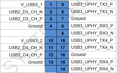
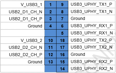
7.5 USB 3.0 Connectors(J8, J9)
4x USB3.0 ports have been terminated on two dual port vertically stacked connector. These 2 ports are backward compatible to USB2.0.
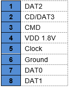
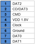
7.5 uSD Connectors(J8, J9)
The daughter board provides a standard Micro SD connector as an additional storage option.
7.6 uSIM Connectors(J8, J9)
The SIM interface from minicard socket is connected to micro SIM card slot.
Last updated