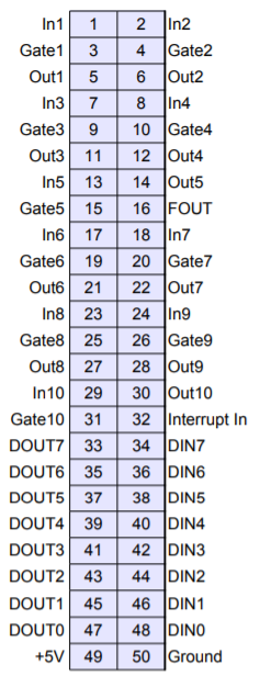
Counter/timer Header Pinout
Connector (J3) is the 50-pin counter/timer interface. The connector connects directly to the FPGA, which implements the functionality of two CTS9513 counter/timer chips.
Ten input and ten output counter/timer signals
Eight input and eight output TTL-level signals
Ten gates
Power and ground
The J3 pins may be configured to pull-up to +5V or pull-down to ground using jumper J8, as describe in Section 4, Board Configuration, Line Pull-up/pull-down Selection.
NOTE: The connector is labeled “Port 1,” which should not be confused with DIO ports A, B and C and the fixed-direction TTL ports.
Signal | Description |
In1-In10 | Ten external clock source lines that may be associated with one of the ten internal counters or FOUT. |
Out1-Out10 | Ten tri-state outputs lines associated with one of the ten internal counters. These may be programmed for pulse, wave or complex duty cycle waveforms |
Gate1-Gate10 | Ten input lines used to control counter behavior. These may also be used as clock or count input sources for the internal counters or the FOUT divider. |
FOUT | FOUT is a general-purpose, auxiliary clock output derived from the 9513 input clock using a programmable divider. |
Interrupt In | External interrupt for external PC/104 bus hardware interrupt operation. |
DOUT0-DOUT7 | Eight general-purpose digital output lines. |
DIN0-DIN7 | Eight general-purpose digital input lines. |
+5V | +5 volt DC from the PC/104 bus. |
Ground | Digital ground from the PC/104 bus. |
Last updated