14.4.2 Page 0: Counter/Timer Control
Page 0, Base + 12 Read/Write Counter/Timer 0/1 D7 - 0
This register is used for both Counter 0 and Counter 1. It is the LSB for both counters. When writing to this register, an internal load register is loaded. Upon issuing a Load command through page 0, base + 15, the selected counter’s LSB register will be loaded with this value. When reading from this register, the LSB value of the most recent Latch command will be returned. The value returned is NOT the value written to this register.
Page 0, Base + 13 Read/Write Counter/Timer 0/1 D15 - 8
This register is used for both Counter 0 and Counter 1. It is the MSB for counter 1 and the middle byte for counter 0. When writing to this register, an internal load register is loaded. Upon issuing a Load command through page 0, base + 15, the selected counter’s associated register will be loaded with this value. For counter 0, it is the middle byte. For counter 1, it is the MSB. When reading from this register, the associated byte of the most recent Latch command will be returned. The value returned is NOT the value written to this register.
Page 0, Base + 14 Read/Write Counter/Timer 0 D23 - 16
This register is used for Counter 0 only. Counter 0 is 24 bits wide, while Counter 1 is only 16 bits wide. When writing to this register, an internal load register is loaded. Upon issuing a Load command through page 0, base+15 for Counter 0, the counter’s MSB register will be loaded with this value. When issuing a Load command for counter 1, this register is ignored. When reading from this register, the associated byte of the most recent Latch command will be returned. The value returned is NOT the value written to this register.
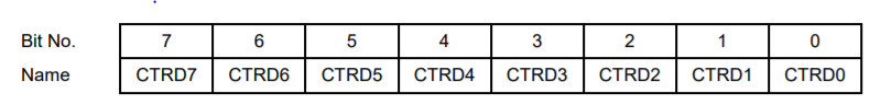
Page 0, Base + 15 Write Counter/Timer Control Register
This register is used to control the counter/timers. A counter is selected with bit 7, and then a 1 is written to any ONE of bits 6 – 0 to select the desired operation for that counter. The other bits and associated functions are not affected. Only one operation can be performed at a time. If more than one of bits 6-0 is set simultaneously, the highest numbered bit will determine the operation to be performed
CTRNO | Counter no., 0 or 1 |
LATCH | Latch the selected counter so that its value may be read. The counter must be latched before it is read. Reading from registers at page 0, base+12 thru base+14 returns the most recently latched value. If you are reading Counter 1 data, read only page 0, base+12 and base+13. Any data in page 0, base+14 will be from the previous Counter 0 access. |
GTDIS | Disable external gating for the selected counter (see GTEN below). |
GTEN | Enable external gating for the selected counter. If enabled, the associated input signal GATE0 or GATE1 controls counting on the counter. If the GATEn signal is high, counting is enabled. If the GATEn signal is low, counting is disabled. |
CTDIS | Disable counting on the selected counter. The counter will ignore input pulses. |
CTEN | Enable counting on the selected counter. The counter will decrement on each input pulse. |
LOAD | Load the selected counter with the data written to page 0, base+12 through base+14 (Counter 0) or page 0, base+12 and base+13 (Counter 1). |
CLR | Clear the current counter (set its value to 0). Counter operation such as count enable or gate enable is not affected by the CLR command. If the counter is enabled it will continue to count input pulses |
Page 0, Base + 15 Read FPGA Revision Code
This register is used to indicate the board ID and data acquisition FPGA revision. The initial production version of Helios reads back ID code 0x70. The code will increment by 1 each time a new revision is released.
REV3-0 | Revision code. This reads back as 0 in the initial production release of the on-board FPGA code and increments by 1 for each subsequent update. |
BID3-0 | Board ID code. This reads back as 7 (b0111) for Helios |
Last updated