17. DIGITAL I/O
This page describes the Digital I/O specification on Gemini carrier card
17.1 DIGITAL I/O specification
Each digital I/O line can be individually configured to set the input or output direction. This enables the Digita I/O pins to be split as input and output. All lines can be individually read or written, enabling I/O peripherals configurations to be customized to suit application requirements. The output pins can be set as open-drain or push-pull.
Digital I/O Specifications | |
Device | CP2112 |
Number of Lines | 8 |
Direction | Bidirectional, Programmable bit by bit |
Input voltage | |
Logic 0: | 0V min: 0.6V max |
Logic 1 | 2.31 min: 3.3V max |
Output Voltage | |
Logic 0: | 0.0V min: 0.6 max @ 25mA output current |
Logic 1 | 2.9V min @-10mA output current: 3.3V max |
Since the Digital I/Os are realized with USB to GPIO expander, the Digital I/Os do not support additional features such as edge detection on input, PWM features on output, etc, but can only be used to write and read logic high & logic low.
The Digital I/O pins are not 5V tolerant.
17.2 DIGITAL I/O Software
The CP2112 USB to I2C bridge is configured to be an HID device so separate drivers are not needed for this device.
Silicon Labs provides an SDK for the CP2112 device which can be used to program the Digital I/Os. Click here to download the SDK for the CP2112 device.
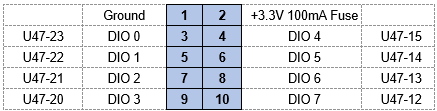
The mapping table below represents DIO signals from CP2112 IC to J33 DIO connector.
Last updated