14.4.1 Main Registers
Base + 0 Write Command Register
This register is used to perform various functions. The register bits are not data bits but instead command triggers. Each function is initiated by writing a 1 to a particular bit. Writing a 1 to any bit in this register does not affect any other bit in this register. For example, to reset the FIFO, write the value 0x10 (16) to this register to write a 1 to bit 4. No other function of the register will be performed. Multiple actions can be carried out simultaneously by writing a 1 to multiple bits simultaneously.
STRTAD | Writing a 1 to this bit starts an A/D conversion (trigger the A/D) when in software-trigger mode (AINTE = 0). The A/D conversion will start and the ADBUSY bit (base+3, bit 7) will go high. When the A/D conversion completes and the data is stored in the FIFO, the STS bit goes low. When AINTE = 1 (base+4, bit 0), the A/D cannot be triggered by writing to this bit. Instead the A/D will be triggered by a signal selected by ADCLK (base+4, bit 5). |
RSTBRD | Writing a 1 to this bit will reset the entire board excluding the D/A, causing all registers on the board to be reset to 0. The effect on the digital I/O is that all ports are reset to input mode, and the logic state of their pins will be determined by the pull-up/pull-down configuration setting selected by the user. All A/D, counter/timer and interrupt functions will cease. However the D/A values will remain constant. |
RSTDA | Writing a 1 to this bit causes the FPGA to send a reset command to the D/A converter. |
RSTFIFO | Reset the FIFO depth to 0. This clears the FIFO so that further A/D conversions will be stored in the FIFO starting at address 0. All FIFO flags are set to their states for empty FIFO (EF = 1, all others = 0). |
CLRT | Writing a 1 to this bit causes the timer interrupt request flip flop to be reset. |
CLRD | Writing a 1 to this bit causes the digital I/O interrupt request flip flop to be reset. |
CLRA | Writing a 1 to this bit causes the analog interrupt request flip flop to be reset. |
Base + 0 Read A/D LSB
If the FIFO is not empty, this register returns the LSB of the A/D value stored at the current FIFO pointer. If the FIFO is empty, reading from this register returns 0.
AD7 – 0 A/D data bits 7 - 0; AD0 is the LSB.
Base + 1 Write Page Register
PG1-PG0 | Page Select (0 - 2): The addresses base+12 to base+15 provide a window into 3 pages of registers, 0-2. Page 3 is undefined and maps back to page 0. |
Base + 1 Read A/D MSB
If the FIFO is not empty, this register returns the MSB of the A/D value stored at the current FIFO pointer and decrements the FIFO depth value by 1 sample. If the FIFO is empty, reading from this register returns 0.
AD15 - 8 A/D data bits 15 – 8; AD15 is the MSB.
Base + 2 Read/Write A/D Channel Register
When this register is written to, the current A/D channel is set to the channel specified by L3-0, so that the next time an A/D conversion is triggered the channel specified by L3-0 will be sampled.
When this register is written to, the WAIT bit (base+3, bit 5) will go high for 10 microseconds to indicate that the analog input circuit is settling. During this time the board will ignore any A/D start command. It is still possible to write to base+3 to configure the analog input circuit during the WAIT period. In this case the WAIT delay is retriggered, so that it will always endure for the full wait period after the last triggering function.
The A/D circuit is designed to automatically increment the A/D channel each time an A/D conversion is triggered. This enables the user to avoid having to write the A/D channel each time. The A/D channel will rotate through the values between L3-0 and H3-0. When channel H3-0 is sampled, the register resets to L3-0.
Reading from this register returns the value previously written to it.
H3-H0 | High channel of channel scan range (HIGH) Ranges from 0 to 15 in single-ended mode, 0 - 7 in differential mode |
L3-L0 | Low channel of channel scan range (LOW) Ranges from 0 to 15 in single-ended mode, 0 - 7 in differential mode. |
It is not required that the High channel be greater or equal to the Low channel. A setting of Low=14 and High=2 is valid. In this case the channel sequence is 14, 15, 0, 1, 2, 14, 15, …
Base + 3 Write Analog Input Gain and Scan Control
When this register is written to, the WAIT bit (base+3, bit 5) will go high for 10 microseconds to indicate that the analog input circuit is settling. During this time the board will ignore any A/D start command. It is still possible to write to base+2 to configure the analog input channel register during the WAIT period. In this case the WAIT delay is re-triggered, so that it will always endure for the full wait period after the last triggering function.
SCANEN | Scan mode enable: 1 Each A/D trigger to cause the board to generate an A/D conversion on each channel in the range LOW – HIGH as defined in Base+2. The ADBUSY bit (base+3, bit 7) stays high during the entire scan. 0 Each A/D trigger to cause the board to generate a single A/D conversion on the current channel. The internal channel pointer will increment to the next channel in the range LOW – HIGH or reset to LOW if the current channel is HIGH. The ADBUSY bit stays high during the A/D conversion. |
ADG1-0 | Analog input gain. The gain is the ratio of the voltage seen by the A/D converter and the voltage applied to the input pin. The gain setting is the same for all input channels. The following table lists the available analog input ranges. Unipolar / bipolar range is selected with the ADPOL bit in page 2 base+13. |
ADG1 | ADG0 | Gain | Unipolar Range | Bipolar Range |
0 | 0 | 1 | 0-10V | +/-10V |
0 | 1 | 2 | 0-5V | +/-5V |
1 | 0 | 4 | 0-2.5V | +/-2.5V |
1 | 1 | 8 | 0-1.25V | +/-1.25V |
Base + 3 Read Analog Input Status
ADBUSY | A/D Busy. 1 = A/D conversion or scan in progress, 0 = A/D is idle. After starting a conversion in software, the program must monitor ADBUSY and wait for it to become 0 prior to reading A/D values. If SCANEN = 0 (single conversion mode), ADBUSY goes high when an A/D conversion is started and stays high until the conversion is finished. If SCANEN = 1 (scan mode enabled), ADBUSY stays high during the entire scan. |
SE/DIFF | Single-ended / Differential mode indicator. 0 = Single-ended, 1 = Differential |
ADWAIT | A/D input circuit status. 1 = A/D circuit is settling on a new value, 0 = ok to start conversion. ADWAIT goes high after the channel register (base+2) or the gain register (base+3) is changed. It stays high for 10 microseconds. The program should monitor this bit after writing to either register and wait for it to become 0 prior to starting an A/D conversion. |
DACBSY | Indicates the DAC is busy updating (approx. 4 µS). 1 = Busy, 0 = Idle. Any writes to the DAC (base+6, base+7, or page 2 base+15) while DACBSY = 1 will be ignored. |
OF | FIFO Overflow bit. This bit indicates that the FIFO has overflowed, meaning that the A/D circuit has attempted to write data to it when it is full. When overflow occurs, the FIFO will not accept any more data until it is reset. Once set, the OF flag remains true until the FIFO is reset, so the application program will be able to determine if overflow has occurred. If overflow occurs, then you must either reduce the sample rate or increase the efficiency of your interrupt routine and/or operating system. |
SCANEN, ADG1-0 | Readback of scan enable and A/D gain settings written to base+2 |
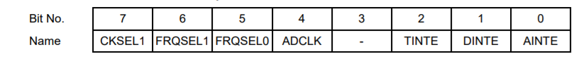
Base + 4 Read/Write Interrupt / Counter Control
Analog output interrupts are not supported on this board.
Multiple interrupt operations may be performed simultaneously. All interrupts will be on the same interrupt level. The user’s interrupt routine must monitor the status bits to know which circuit has requested service. After processing the data but before exiting, the interrupt routine must then clear the appropriate interrupt request bit using the register at base+0.
CKSEL1 | Clock source selection for counter/timer 1: 0 = internal oscillator, frequency selected by FRQSEL1 1 = external clock input CLK1 (DIOCTR must be set to 1 to enable CLK1 input on J17) |
FRQSEL1 | Input frequency selection for counter/timer 1 when CKSEL1 = 1: 0 = 10MHz 1 = 100KHz |
FRQSEL0 | Input frequency selection for counter/timer 0. 0 = 10MHz 1 = 1MHz |
ADCLK | A/D trigger select when AINTE = 1: 0 = internal clock output from counter/timer 0 1 = external signal on pin 25 of the analog I/O connector J17. |
TINTE | Enable timer interrupts: 1 = enable, 0 = disable |
DINTE | Enable digital I/O interrupts: 1 = enable, 0 = disable |
AINTE | Enable analog input interrupts: 1 = enable, 0 = disable When AINTE = 0. the A/D is triggered only by writing a 1 to the ADSTART bit at base+0. When AINTE = 1, the A/D cannot be triggered by setting the ADSTART bit at base+0. Instead the A/D trigger comes from the hardware source selected by the ADCLK bit. |
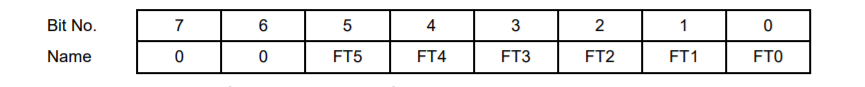
Base + 5 Write FIFO Threshold / FIFO Threshold X8
Basic Mode: EXFIFO = 0 (See Register Description for page 2, base+12)
FT5–0 | FIFO threshold. When the number of A/D samples in the FIFO reaches this number, the board will generate an interrupt and set AINT high (base+7, bit 4) when AINTE=1. The valid range is 1-48. If the value written is greater than 48, then 48 will be used. If the value written is 0, then 1 will be used. |
Enhanced Mode: EXFIFO = 1 (See Register Description for page 2, base+12)
FT10–03 | FIFO threshold (upper 8 of 11 bits). The lower 3 bits are 000. The FIFO threshold will be set to 8x the number programmed into this register (left shift 3 bits). When the number of A/D samples in the FIFO reaches the threshold, the board will generate an interrupt and set AINT high (base+7, bit 4) when AINTE=1. The valid range is 1 – 255, corresponding to a FIFO threshold of 8-2040. When EXFIFO is set to 1 the FIFO threshold is set automatically to 1024. |
Base + 5 Read FIFO Threshold / FIFO Depth LSB
Basic Mode: EXFIFO = 0 (See Register Description for page 2, base+12)
FT5-0 Readback of the programmed FIFO threshold value
Enhanced Mode: EXFIFO = 1 (See Register Description for page 2, base+12)
FD07-00 | FIFO depth. Readback of the lower 8 bits of the number of A/D values currently stored in the FIFO |
Base + 6 Write DAC LSB
DA7–0 | D/A data bits 7 - 0; This register stores the DA LSB in both 12 and 16-bit modes |
Base + 6 Read A/D Channel and FIFO Status
Basic Mode: EXFIFO = 0 (See Register Description for page 2, base+12)
FD5–0 | FIFO depth. Readback of the number of A/D values currently stored in the FIFO. |
Enhanced Mode: EXFIFO = 1 (See Register Description for page 2, base+12)
FD11–08 | Readback of the upper 4 bits of the number of A/D values currently stored in the FIFO. |
OF | FIFO Overflow flag. 1 = FIFO has overflowed, meaning that the A/D circuit has attempted to write data to it when it is full. The OF flag is set whenever FF = 1 and an A/D conversion completes (STS goes high then low). 0 = FIFO has not overflowed. |
FF | FIFO Full Bit. 0 = FIFO is not full; the FIFO is able to accept data from the A/D circuit. 1 = FIFO is full; the next conversion will result in an overflow |
HF | FIFO Half Full Bit. 0 = the FIFO is less than half full. 1 = the FIFO is half full or greater. |
EF | FIFO Empty. 0 = the FIFO still has data. 1 = the FIFO is empty. |
Base + 7 Write DAC MSB
When this register is written, the D/A channel selected by DACH1-0 will be loaded using the currently stored D/A value in the registers selected by DAMODE. If DASIM=0, the D/A will then be updated. If DASIM=1, the D/A will not be updated.
DACH1–0 | D/A channel, 0-3. |
DA11–8 | D/A bits 11 – 8 when operating the D/A in 12-bit mode. These bits are ignored for 16-bit mode. |
Base + 7 Read Analog Operation Status
When any of the bits 6–4 are 1, the corresponding circuit is requesting interrupt service. The interrupt routine must poll these bits to determine which circuit needs service and then act accordingly.
TINT | Timer interrupt status: 1 = interrupt pending, 0 = interrupt not pending |
DINT | Digital I/O interrupt status: 1 = interrupt pending, 0 = interrupt not pending. |
AINT | Analog input interrupt status: 1 = interrupt pending, 0 = interrupt not pending. |
ADCH3-0 | Current A/D channel. This is the channel that will be sampled on the next A/D conversion |
Base + 8 Read / Write Digital I/O Port A
This register is used for digital I/O on port A. When port A is in output mode, the output pins DIO A7-0 on data acquisition connector J17 will be set to the values in this register, and reading this register will read back the programmed value. When port A is in input mode, this register will read back the logic levels on pins DIO A7-0, and writing to this register will have no effect. The direction of port A is controlled by the DIO control register at base+11.
Base + 9 Read / Write Digital I/O Port B
This register is used for digital I/O on port B. When port B is in output mode, the output pins DIO B7-0 on data acquisition connector J17 will be set to the values in this register, and reading this register will read back the programmed value. When port B is in input mode, this register will read back the logic levels on pins DIO B7-0, and writing to this register will have no effect. The direction of port B is controlled by the DIO control register at base+11.
Base + 10 Read / Write Digital I/O Port C
This register is used for digital I/O on port C. It operates in similar fashion to ports A and B, except that 4 pins on the I/O connector serve a different purpose based on the value of DIOCTR in base+11.
When DIOCTR=0, the behavior is as follows: When port C is in output mode, the output pins DIO C7-0 on data acquisition connector J17 will be set to the values in this register, and reading this register will read back the programmed value. When port C is in input mode, this register will read back the logic levels on pins DIO C7-0, and writing to this register will have no effect. The direction of port C is controlled by the DIO control register at base+11.
When DIOCTR=1, the behavior of bits C3-0 is the same as above, and bits C7-4 are not functional. Instead, the corresponding I/O pins on connector J17 are used for counter/timer signals as described in base+11 below.
Base + 11 Read / Write Digital I/O and D/A Control Register
DIOCTR | Selects counter I/O signals or digital I/O lines on 4 pins on the data acquisition I/O connector J17 |
J17 Pin No. | DIOCTR = 1 | DIOCTR = 0 |
21 | Gate0 | DIOC4 |
22 | Gate1 | DIOC5 |
23 | Clk1 | DIOC6 |
24 | Out0 | DIOC7 |
If DIOCTR = 0, then the direction of these pins is controlled by DIRCH.
DAMODE | 16/12-bit DAC mode. This bit should only be set for custom models of Helios with a 16-bit DAC installed. This bit defines where the high bits of the D/A value are to be found when loading the D/A. Regardless of whether the installed D/A is 12 bits or 16 bits, the data value written to the D/A is always 16 bits in length. For a 12-bit D/A, the 12-bit data is left-justified in this 16-bit word, and the lowest 4 bits are always 0000. 0 D/A is being used in 12-bit mode (standard configuration). The data register at Base+5 contains the high bits 11-8 of the 12-bit D/A value. 1 D/A is being used in 16-bit mode (custom configuration). The data register at Page 2 Base+15 contains the high bits 15-8 of the 16-bit D/A value. |
DASIM | D/A simultaneous update control. This bit determines when the D/A is updated. 0 When Base+6 is written, the D/A data is loaded into the D/A and the update command is sent immediately afterwards. 1 When Base+6 is written, the 12/16-bit values will be loaded into the D/A converter but the update command will not be issued. Instead, a read of the register at Page 2, Base+15 will cause the update of the D/A converter. |
DIRA | Port A direction. 0 = output, 1 = input |
DIRB | Port B direction. 0 = output, 1 = input |
DIRCH | Port C bits 7-4 direction: 0 = output, 1 = input. This bit has no effect if DIOCTR=1. |
DIRCL | Port C bits 3-0 direction: 0 = output, 1 = input |
Last updated